ACSIN-16 & ICSPM34
October 19-23, 2026, Arcrea HIMEJI, JapanSchedule
Detailed scientific program available!
View Full Schedule
| Oct 19 Mon | Oct 20 Tue | Oct 21 Wed | Oct 22 Thu | Oct 23 Fri |
|---|---|---|---|---|
| Opening Plenary | Plenary | Plenary | Plenary | |
| Award lecture, ceremony, photo | Parallel sessions | Parallel sessions | Parallel sessions | |
| Lunch (Luncheon seminors) | Lunch (Luncheon seminors) | Excursion | Lunch (Buffet) | |
| Parallel sessions | Parallel sessions | Parallel sessions & Closing | ||
| Parallel sessions | Parallel sessions | |||
Welcome reception | Poster Session | Poster Session | Banquet |
Plenary Speakers
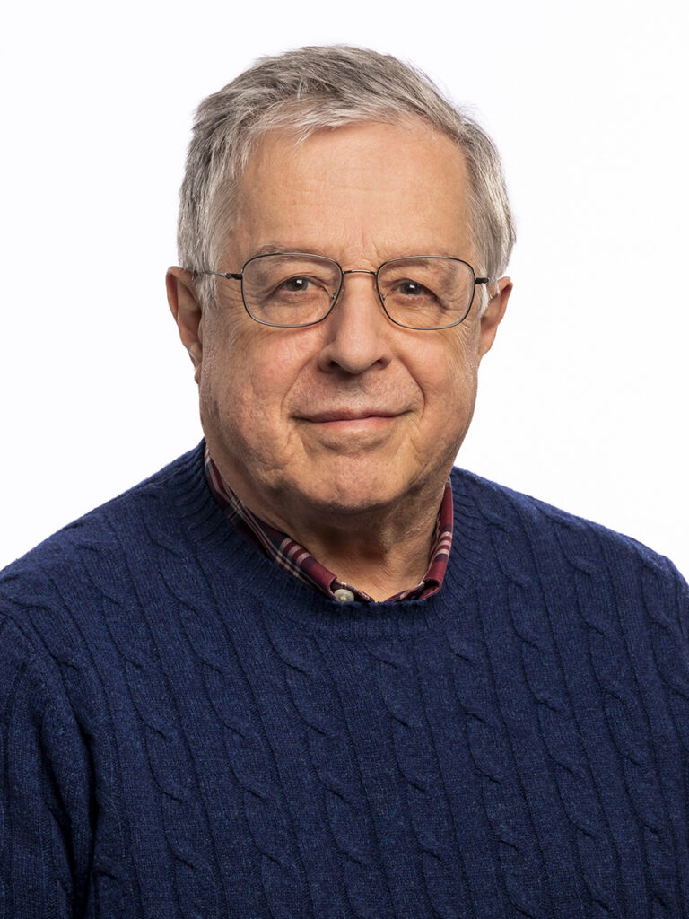 Car, Roberto (Princeton Univ, USA)
https://chemistry.princeton.edu/faculty-research/faculty/roberto-car/ open_in_new
Molecular simulation in the age of artificial intelligence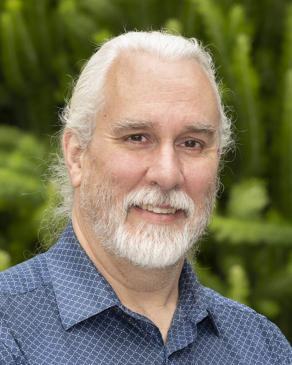 Fuhrer, Michael S. (Monash University, Australia)
https://research.monash.edu/en/persons/michael-fuhrer/ open_in_new
Reconfigurable Quantum Materials for Low-energy Electronics George, Steven M. (Univ. of Colorado Boulder, USA)
https://www.colorado.edu/lab/georgegroup/ open_in_new
Thermal Atomic Layer Etching of High K and Semiconductor Metal Oxides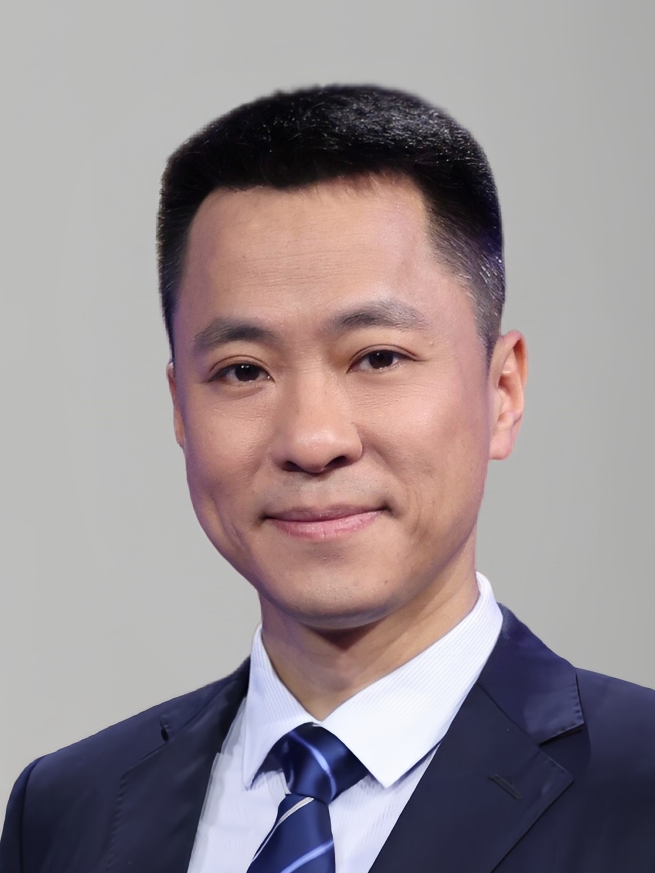 Jiang, Ying (Peking University, China)
http://jiang.pku.edu.cn/ open_in_new
Water and ice under extreme confinement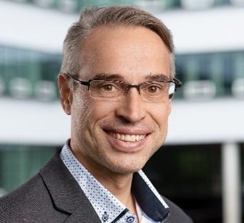 Nijhuis, Christian (University of Twente, Netherland)
https://people.utwente.nl/c.a.nijhuis open_in_new
Molecular-Scale Information Processing with Dynamic Molecular Switches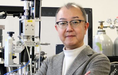 Ohta, Hiromichi (Hokkaido University, Japan)
https://functfilm.es.hokudai.ac.jp/ open_in_new
From Oxide Electronics to Thermo-iontronics: Controlling Electrons, Phonons, and Ions in Metal Oxides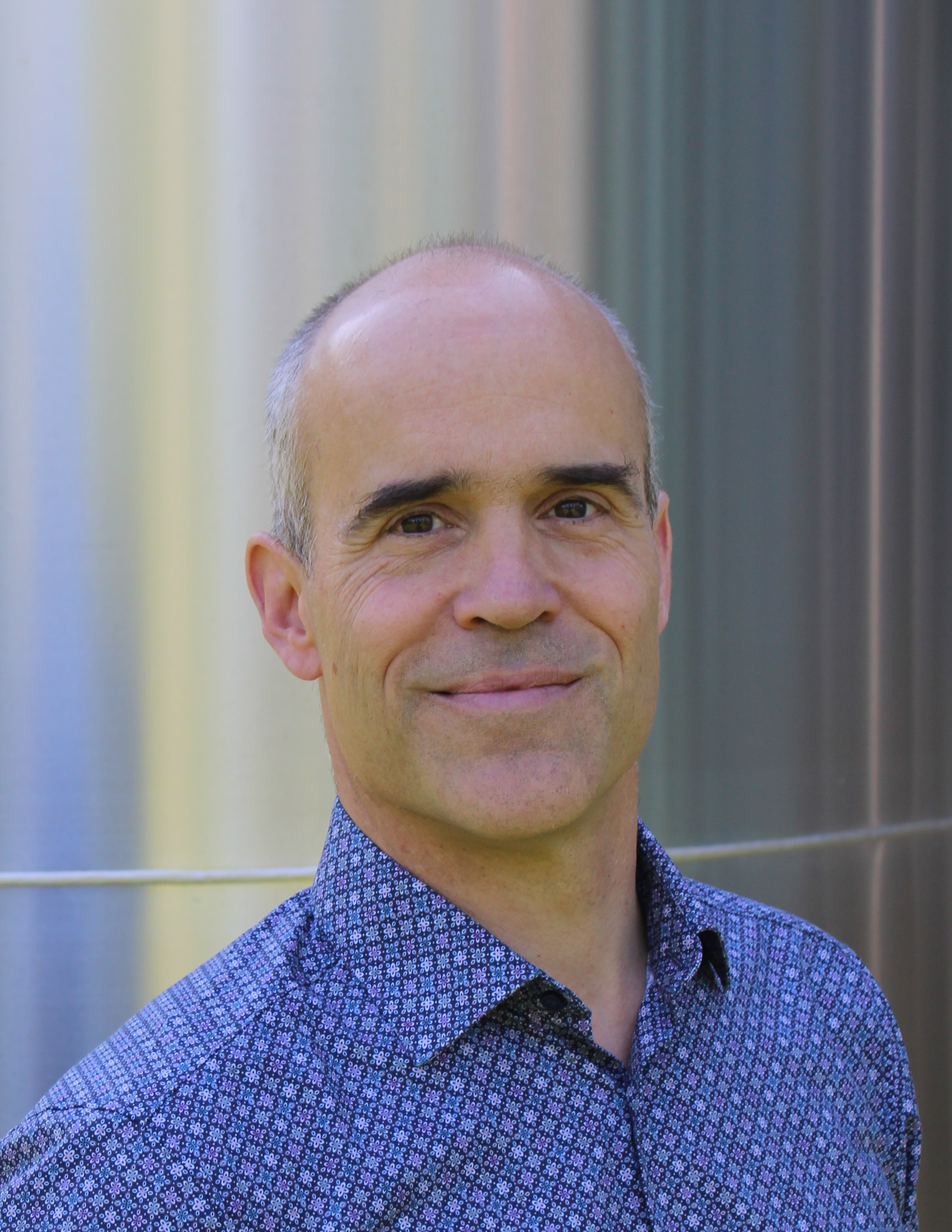 Repp, Jascha (University Regensburg, Germany)
https://www.uni-regensburg.de/physics/repp/home/ open_in_new
Non-equilibrium at atomic scales: shaken or stirred… and scanned.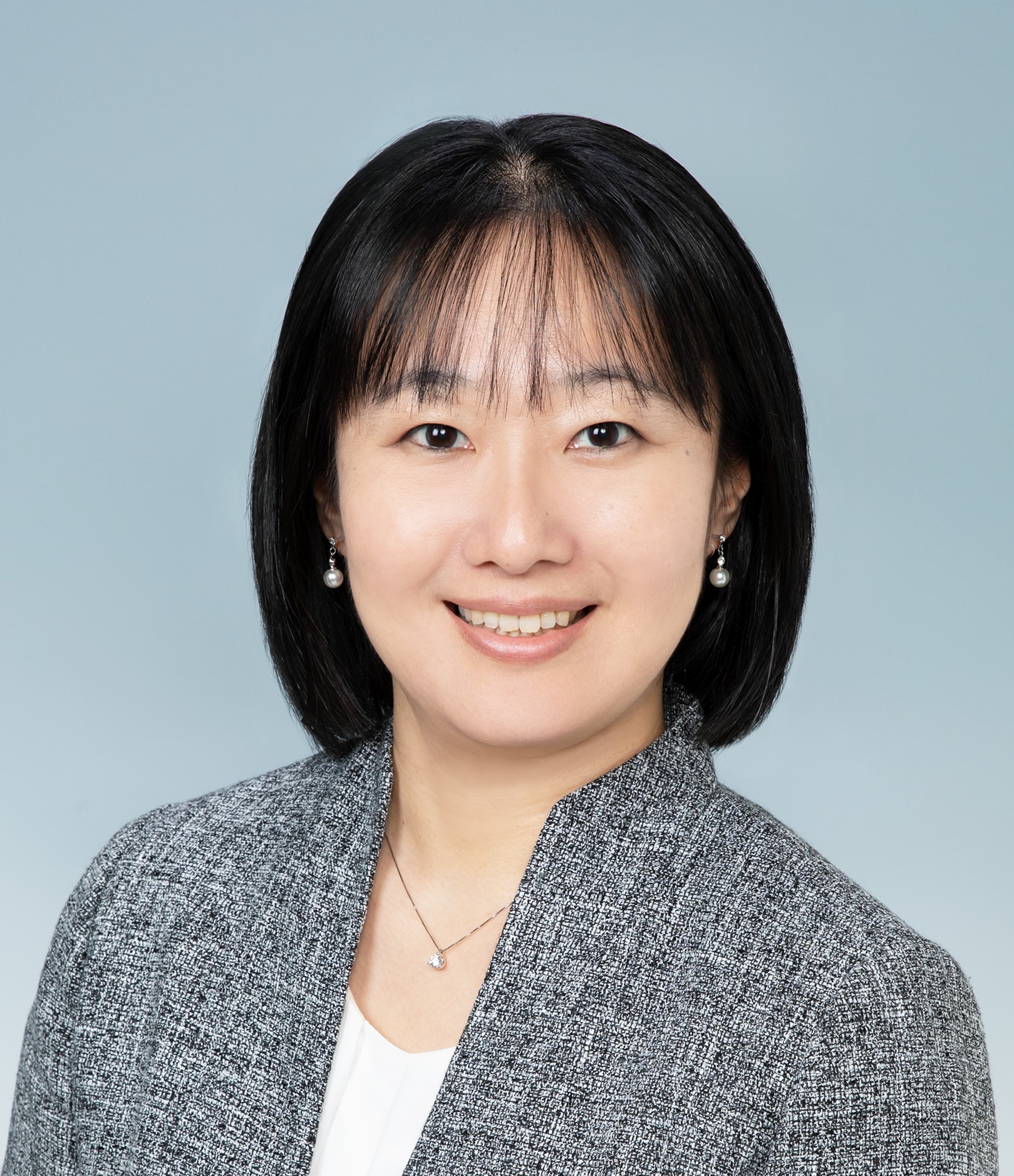 Tada, Mizuki (Nagoya University, Japan)
https://cat.chem.nagoya-u.ac.jp/ open_in_new
Unlocking the Complexity of Solid Materials through Operando Spectroimaging
Invited Speakers
- Fabrication of Nanostructures and Films
- Ago, Hiroki (Kyushu University, Japan) open_in_new
Controlled synthesis and transfer of 2D materials for electronic applications - Chu, Ying-Hao (National Tsing Hua University, National Yang Ming Chiao Tung University, Academia Sinica, Taiwan) open_in_new
Van der Waals Epitaxy of Bi2O2Se for Advanced Semiconductor Devices - Fukata, Naoki (NIMS, Japan) open_in_new
Functionalized Semiconductor Nanostructures for Future Electronic- and Energy-related Devices - Kobayashi, Takashi (Riken, Japan) open_in_new
Characterization and operations of academically developed silicon 12- qubit devices - Mizuguchi, Masaki (Nagoya University, Japan) open_in_new
Control of Anomalous Nernst Effect in Nano-porous Magnetic Thin Films - Pierre, Seneor (Université Paris-Saclay, CNRS, Thales, France) open_in_new
2D Spintronics: From Spinterface to Band Engineering of VDW Heterostructures - Qing-Tai , Zhao (Forschungszentrum Julich GmbH, Germany) open_in_new
Silicon devices for neuromorphic computing - Tomioka, Katsuhiro (Hokkaido University, Japan) open_in_new
Vertical III-V Nanowire Multi-Mode Transistor for Circuit Application
- Ago, Hiroki (Kyushu University, Japan) open_in_new
- Surface and Interface Engineering for Electronic Devices
- Jia, Baohua (RMIT University, Australia) open_in_new
Engineering Atomaterials for Sustainability Devices - Kim, Young Keun (Korea University, Korea) open_in_new
3D Chiral Spintronics: Spin-Selective Transport through Chiral Magnetic Nanohelices - Sakai, Akito (The University of Tokyo, Japan) open_in_new
Intrinsic transverse thermoelectric effect in topological magnets and its application to heat flow sensors - Takahashi, Takanori (Nara Institute of Science and Technology, Japan) open_in_new
Atomic layer deposited oxide semiconductor nanosheet for integrated device applications
- Jia, Baohua (RMIT University, Australia) open_in_new
- Electrons, Spins, Photons, Phonons in 1D, 2D Materials
- Du, Yi (Beihang University, China)
Design and Exploration of 2D Quantum Matters with Exotic Properties - Hasegawa, Shuji (University of Tokyo, Japan)
Structure and Transport Property of Epitaxial Graphene - Markus, Donath (Munster University, Gernany) open_in_new
Exotic Spin Textures in Unoccupied Two-Dimensional Electron States - Rong, Xiang (Zhejiang University, China) open_in_new
One-dimensional van der Waals nanotubes and heterostructures - Shengxi, Huang (Rice University, USA) open_in_new
Improving single photon emission from vdW materials via atomic engineering - Vincent, Tung (The University of Tokyo, Japan) open_in_new
Emerging 2D P-Type Semiconductors
- Du, Yi (Beihang University, China)
- Soft Materials, Synthetic and Biological
- Cartagena-Rivera, Alexander (NIH, USA) open_in_new
Glycocalyx Desialylation Remodels Surface Mechanics to Potentiate Cytotoxic T Cell Responses in Pancreatic Ductal Adenocarcinoma - Felix, Rico (IUNSERM, France) open_in_new
Universal dynamics of coiled coils revealed by high-speed atomic force microscopy - Ichiki, Takanori (The University of Tokyo, Japan) open_in_new
Surface-Potential Analysis of Extracellular Vesicles
- Cartagena-Rivera, Alexander (NIH, USA) open_in_new
- Surface Characterization, Methods and Instruments
- Höfer, Ulrich (Department of Physics, University of Marburg, Germany) open_in_new
Time-resolved photoemission orbital tomography of molecular excitons - Kim, Yousoo (, Korea)
Energy Flow among Quantum States in a Single-Molecule STM Junction - Lin, Meng-Kai (Department of Physics, National Central University, Taiwan) open_in_new
Moiré-Driven Quantum Phenomena in Ultrathin van der Waals Heterostructures - Torelli, Piero (Italian National Research Council, Italy) open_in_new
Ambient Pressure soft-XAS for surface reactivity investigation
- Höfer, Ulrich (Department of Physics, University of Marburg, Germany) open_in_new
- Scanning Probe Microscopy
- Björk, Jonas (Docent in Materials Science, Linköping University, Sweeden) open_in_new
Toward Predictive Modeling of On-Surface Chemical Reactions - Jelinek, Pavel (Institute of Physics of the Czech Academy of Sciences, Czech) open_in_new
Scanning probe microscopy of strongly correlated molecules on surfaces - Le Lay, Guy (, France)
The Booming Field of Xenestronics - Phark, Soo-hyon (Center for Quantum Nanoscience (QNS) of Institute for Basic Science, Korea) open_in_new
Single- and Two-Qubit Quantum Gates to Bottom-up Crafted Spin Qubits - Ruffieux, Pascal (EMPA, Switzerland) open_in_new
Nanographene Spin Chains - Setvin, Martin (Charles University, Czech) open_in_new
Localized charges in ionic lattices: Imaging the Position and Dynamics - Shiotari, Akitoshi (Fritz-Haber Institute of the Max-Planck Society, Germany) open_in_new
Picocavity-based Tip-enhanced Raman Spectroscopy for Single Molecules - Taucer, Marco (CBN Nano Technologies, Canada)
Inverted-Mode STM for Atomically Precise Fabrication on Silicon
- Björk, Jonas (Docent in Materials Science, Linköping University, Sweeden) open_in_new
- Surfaces under Vacuum, Vapor, Plasma
- Chae, Heeyeop (Sungkyunkwan University, Korea) open_in_new
Plasma-Enhanced Atomic Layer Etching of Metals and Dielectrics for Semiconductor Device Processing - Kim, Sang-Woo (Yonsei University, Korea) open_in_new
Triboelectric Medicine: Shaping the Future of Biomedical Innovation - Ohta, Takayuki (Meijo University, Japan)
Deposition of metal oxide semiconductor materials for MOS transistors by high-power impulse magnetron sputtering
- Chae, Heeyeop (Sungkyunkwan University, Korea) open_in_new
- Interfaces Buried in Liquid, Solid
- Du, He-Yun (Ming Chi University of Technology, Taiwan) open_in_new
Materials, Scanning Probe Microscopy, and Reaction Simulation for Local Electrochemical Activity at Buried Interfaces - Hosono, Nobuhiko (University of Tokyo, Japan) open_in_new
AFM in MOF Research: From High-Resolution Imaging to Nanomechanics - Ivanistsev, Vladislav (University of Latvia, Latvia) open_in_new
Effect of Ionic Size on Structure and Dynamics at Solid–Liquid Interface
- Du, He-Yun (Ming Chi University of Technology, Taiwan) open_in_new
- (Symposium) Atomically Controlled Materials for Quantum Applications
- Butler, Christopher (RIKEN, Japan)
Imaging the Atomic-Scale Intertwining of Charge and Spin in an Itinerant Skyrmion Magnet - Chen, Lan (Insititute of Physics, Chinese Academy of Sciences, China) open_in_new
Room-Temperature Two-Dimensional Multiferroic Metal with Strong Magnetoelectric Coupling - Fu, Yingshuang (Huazhong University of Science & Technology, China) open_in_new
Atomic-scale insight into excitonic condensation in Ta2Pd3Te5 and HfTe2 - Loth, Sebastian (University of Stuttgart, Germany) open_in_new
Atomic-scale magnetism at the quantum-classical divide - Sessi, Paolo (Max Planck Institute for Solid State Research, Germany) open_in_new
Interfacing Magnetism and Superconductivity: Visualizing Interactions from 0D to 2D - Ugeda, Miguel (Ikerbasque Research, Spain) open_in_new
Coexistence of spatially decoupled unconventional superconducting condensates in 4Hb-TaSSe - Weber, Bent (Nanyang Technological University, Singapore) open_in_new
- Butler, Christopher (RIKEN, Japan)
- (Symposium) Machine Learning for Atomical Control
- Akai, Megumi (Osaka University, Japan) open_in_new
Exploring Material Dynamics for Physical Neuromorphic Computing - Farhi, Emmanuel (Soleil Synchrotron (French National Centre for Scientific Research), France) open_in_new
From Data Deluge to Intelligent Discovery: GRADES’ Software Ecosystem, Data Platforms, and AI-Driven Frontiers at Synchrotron SOLEIL - Lee, Jung-Hoon (Korea Institute of Science and Technology, Korea) open_in_new
AI-Based Inverse-Design Technology for Materials Discovery - Mizoguchi, Teruyasu (The University of Tokyo, Japan) open_in_new
AI for Atomistic Materials Understanding: From Spectroscopy to Generative Design
- Akai, Megumi (Osaka University, Japan) open_in_new
- (Symposium) Quantum Beams for Atomical Control
- Hla, Saw Wai (Ohio University / Argonne National Laboratory, USA) open_in_new
X-ray Spectroscopy and Microscopy of Individual Atoms inside a Molecule - Kanda, Sohtaro (KEK, Japan) open_in_new
Low-Energy Muons for Probing Surfaces and Interfaces - Kotakoski, Jani (University of Vienna, USA) open_in_new
Atomically-precise Structures Tailored within 2D Materials - Tsujikawa, Yuki (Keio University, Japan)
Observation of unexpected 2D copper boride at a surface and exotic states in the internal 1D boron
- Hla, Saw Wai (Ohio University / Argonne National Laboratory, USA) open_in_new
- (Symposium) Atomically Controlled Materials for Carbon Neutrality
- Iguchi, Shoji (Kyoto University, Japan) open_in_new
Macrocyclic Cobalt Complex as a Cathode Catalyst for CO2 Electrolysis - Ikeda, Katsuyoshi (Nagoya Institute of Technology, Japan) open_in_new
Hydrogen evolution reaction using proton permeability of atomically thin monolayer graphene - Kitta, Mitsunori (AIST, Japan) open_in_new
Seeing is Believing: Visualizing Battery Interfaces from Atoms to Cells - Nohira, Toshiyuki (Kyoto University, Japan) open_in_new
Fluoride Shuttle Batteries Using Ionic Liquids and Electrolytic Synthesis of Diamond for Carbon Neutrality
- Iguchi, Shoji (Kyoto University, Japan) open_in_new
Presentation Guide
Oral Presentation Guide
| Category | Talk | Discussion | Total |
|---|---|---|---|
| Plenary | 40 min | 5min | 45 min |
| Invited | 25 min | 5min | 30 min |
| Contributed | 10 min | 5min | 15 min |
All the session rooms will be equipped with a PC running Windows (not Mac), LCD projector (maximum resolution 1920x1200) with a VGA cable (D-sub 15 pin), 16:9 aspect ratio screen, laser pointer, and microphone. If you display your presentation in a 4:3 format, the presentation will fill the screen from top to bottom, and will display with black bars on either side of the 16:9 screen.
Poster Presentation Guide
Schedule
The poster sessions will be held at Exhibition Hall on the ground floor.
- Oct20P-xxx: 17:30 - 19:30, Oct. 20 (Tue)
- Oct21P-xxx: 17:30 - 19:30, Oct. 21 (Wed)
Poster size, set-up and removal
- Poster panels are 2,100 mm in height by 900 mm in width.
- Your poster number will be displayed in advance on the poster panel.
- Poster should be mounted during the designated time and date.
- Oct20P-xxx: from 12:30, Oct. 20 (Tue)
- Oct21P-xxx: from 12:30, Oct. 21 (Wed)
- Poster should be removed at the end of the session
- The material for poster mounting will be supplied. No other materials should be used.